Semiconductor materials can be engineered to have dramatically different electrical and optical properties compared to their bulk counterpart. This is done by making them extremely small to induce quantum confinement. If this could be done in silicon, it could potentially lead to efficient light emission and infrared absorption beyond its native bandgap. Although this is routinely done in III-V semiconductors using quantum wells, it has been nearly impossible in silicon due to a lack of lattice-matched alternate materials.
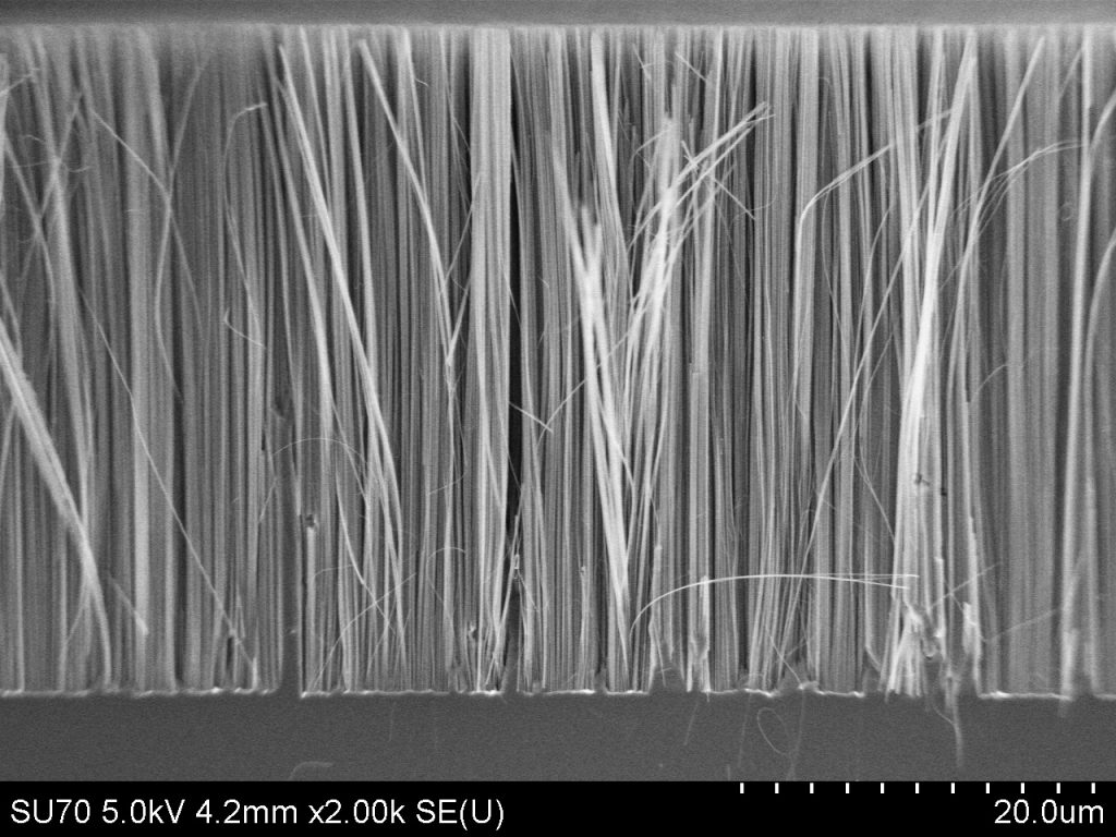
Our approach is based on creating free-standing sheets of ultra-thin silicon (which we call quantum walls). This is done by chemically etching a single-crystal silicon using a method known as Metal-Assisted-Chemical-Etching (MACE). Metals such as gold, silver and platinum can catalyze the etch process in a solution of HF and hydrogen peroxide. The novelty of our approach is that we use a self-assembled network of metal atom. This is created from an ultra-thin film of metal below its percolation threshold. The dimensions of this network is largely determined by the type of metal and the substrate temperature during deposition. Subsequent etching leads to 5-10nm wide sheets of silicon to depths as much as 50um (aspect ratios greater than 10,000). Results show unusual infrared absorption in these structures.


Publications
1.
Joshua M. Duran and Andrew Sarangan. “Fabrication of ultrahigh aspect ratio silicon nanostructures using self-assembled gold metal-assisted chemical etching”. Journal of Micro/Nanolithography, MEMS, and MOEMS, 16(1):014502, 2017. doi:10.1117/1.JMM.16.1.014502
2.
J. Duran and A. Sarangan. “Infrared absorption in MacEtch fabricated silicon quantum walls”. 2016 IEEE Photonics Conference, IPC 2016, 2017. doi:10.1109/IPCon.2016.7831057