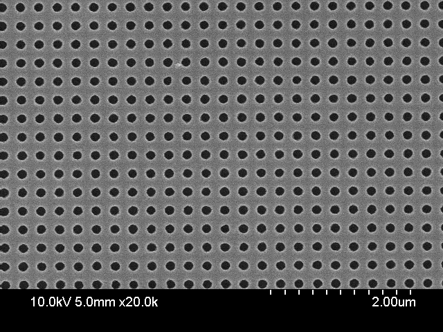
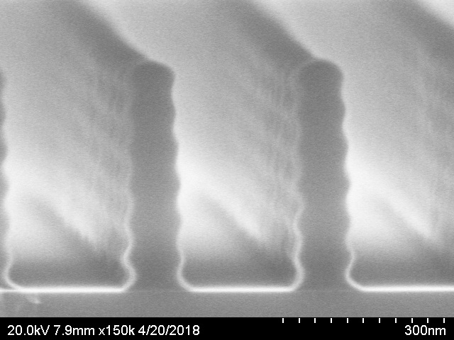
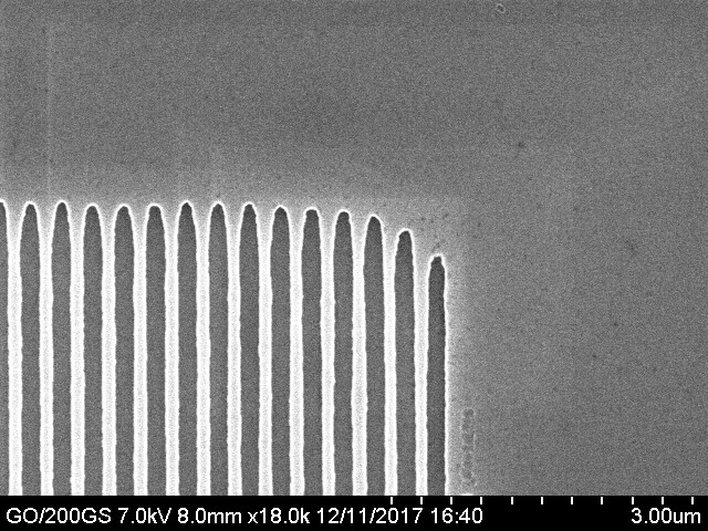
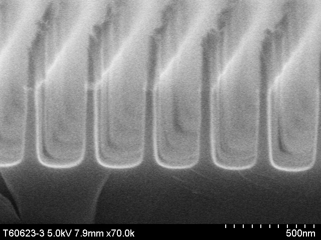
Interference lithography is a technique for creating very small periodic structures without the limitations of conventional lithographic systems. We can easily reach the diffraction limit without having to use high-numerical aperture optics, and the depth of focus is unlimited. We can make one and two dimensional periodic structures with features as small as 100nm over several square inches of area. The limitation is that it can only produce periodic structures. However, this is not as limiting as it may appear at first. The critical steps in a CMOS processes, i.e., gate definitions, are in fact done in a periodic configuration.
Currently we are using this technique to make wiregrid polarizers, diffraction gratings, waveguide couplers as well as nanopatterned templates for other applications such as crystal growth.
The system uses a 266nm deep-UV laser with a Lloyd’s mirror configuration. By rotating the stage, we can make periods ranging from 200nm to 1000nm. The resist is then used to etch into the underlying structure. Alternatively, lift-off patterning is also used. We can also use a masked system in combination with laser intrference. This allows us to create pixel polarizers, which are useful components in imaging polarimetry.


Publications
1.
David Lombardo, Piyush Shah, and Andrew Sarangan. “Single step fabrication of nano scale optical devices using binary contact mask deep UV interference lithography”. Optics Express, 27(16):22917, 2019. doi:10.1364/OE.27.022917
2.
David Lombardo, Piyush Shah, Pengfei Guo, and Andrew Sarangan. “Deep-UV interference lithography combined with masked contact lithography for pixel wiregrid patterns”. Proc. SPIE – The International Society for Optical Engineering, volume 9777, page 97771N, 2016. doi:10.1117/12.2219484
3.
Chenhao Wan, David Lombardo, Andrew Sarangan, and Qiwen Zhan. “Geometric-Phase Polarization Fan-out Grating Fabricated with Deep-UV Interference Lithography”. Journal of Physics: Conference Series, 844(1):012028, 2017. doi:10.1088/1742-6596/844/1/012028
4.
Chenhao Wan, David Lombardo, Andrew Sarangan, and Qiwen Zhan. “High efficiency geometric-phase polarization fan-out grating on silicon”. Optics Express, 25(20):24559, 2017. doi:10.1364/OE.25.024559
5.
Junxin Wang, Yun Zhao, Imad Agha, and Andrew M. Sarangan. “SU-8 nanoimprint fabrication of wire-grid polarizers using deep-UV interference lithography”. Optics Letters, 40(19):4396, 2015. doi:10.1364/OL.40.004396
6.
Junxin Wang and Andrew M. Sarangan. “Nanoimprint fabrication of wiregrids micro-polarizers in near infrared spectra using SU-8 as an intermediate film”. Proceedings of SPIE – The International Society for Optical Engineering, volume 9170, page 917010, 2014. doi:10.1117/12.2061230
7.
Zhi Wu, Andrew M. Sarangan, and Qiwen Zhan. “Fabrication and characterization of long range surface plasmon devices based on metallic subwavelength gratings”. Proceedings of SPIE – The International Society for Optical Engineering, volume 8096, page 80962L, 2011. doi:10.1117/12.893133
8.
Alex Watson, Yu Wang, Zhi Wu, and Andrew Sarangan. “Fabrication of wiregrid micropolarizers for imaging from visible to infrared wavelengths”. IEEE Photonic Society 24th Annual Meeting, pages 99–100. IEEE, 2011. doi:10.1109/PHO.2011.6110444
9.
Andrew M. Sarangan, Aziz Mahfoud, Zhi Wu, Qiwen Zhan, David P. Forrai, Darrel W. Endres, John W. Devitt, Robert T. Mack, and James S. Harris. “Wiregrid micro-polarizers for mid-infrared applications”. Proceedings of SPIE – The International Society for Optical Engineering, volume 6959, page 695915, 2008. doi:10.1117/12.778028
10.
Aziz Mahfoud Familia, Andrew Sarangan, and Thomas R. Nelson. “Optically pumped photonic crystal polymer lasers based on [2-methoxy-5-(2’-ethylhexyloxy)- 1,4-phenylenevinylene]”. Optics Express, 13(8):3136, 2005. doi:10.1364/OPEX.13.003136